


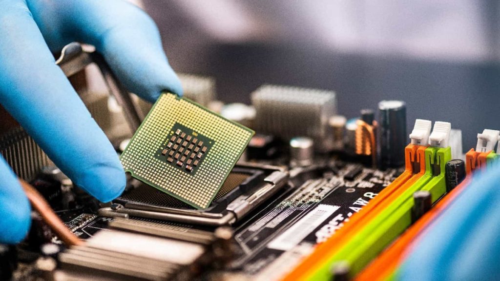
BGA, or Ball Grid Array, is one of the surface-mount packaging technologies most commonly found in integrated circuits. This has recently been in high demand within the structure of the electronics industry, especially when talking about applications that require high-density component placement on printed circuit boards. The article explores the 9 main benefits of using ball grid array when designing and manufacturing a printed circuit board (PCB).
Benefits Of Using Ball Grid Array No. 1 – Increased Connection Density
Contents
- Benefits Of Using Ball Grid Array No. 1 – Increased Connection Density
- Benefits Of Using Ball Grid Array No. 2 – Improved Electrical Performance
- Benefits Of Using Ball Grid Array No. 3 – Enhanced Thermal Performance
- Benefits Of Using Ball Grid Array No. 4 – Reliability and Durability
- Benefits Of Using Ball Grid Array No. 5 – Simplified PCB Design and Manufacturing
- Benefits Of Using Ball Grid Array No. 6 – Flexibility in Design and Rework
- Benefits Of Using Ball Grid Array No. 7 – Cost-Effectiveness at Scale
- Benefits Of Using Ball Grid Array No. 8 – Compatibility with Advanced Technologies
- Benefits Of Using Ball Grid Array No. 9 – Improved Testability
One of the primary advantages of BGA is its ability to provide a significantly higher connection density compared to other packaging technologies…
Maximum I/O count: Due to space availability, hundreds or even thousands of connections can be supported by a BGA package. This is very useful when the integrated circuit is complex, such as in a microprocessor, FPGA, or ASIC application, which needs a large number of inputs and outputs.
Space efficiency: Since the bottom surface of the BGA package is totally utilised for the connections, unlike peripheral-leaded packages where the connections are limited to being only on the edges, it enables much better utilisation of the real estate on a PCB.
Miniaturisation: High interconnection density provided by BGAs enables the designing of less sizable and more compact electronic devices, which is especially important in big industries like mobile electronics, wearables, and IoT devices.
Benefits Of Using Ball Grid Array No. 2 – Improved Electrical Performance
BGA packages offer several electrical performance benefits and because of the ball grid design in the layout, much shorter and more direct connections can be made between the chip and the PCB. Where the signal lengths are reduced, the following can be expected…
Lower inductance
- Reduced signal propagation delays
- Improved signal integrity
- Better power distribution
- Reduced Crosstalk
Benefits Of Using Ball Grid Array No. 3 – Enhanced Thermal Performance
Thermal management is crucial in electronic designs, and BGAs offer several advantages in this area…
Improved Heat Dissipation: Many BGA packages incorporate a heat spreader or have a direct thermal path to the PCB, allowing for more efficient heat dissipation from the chip.
Uniform Heat Distribution: The array of solder balls provides multiple thermal paths, resulting in more uniform heat distribution across the package and the PCB.
Integration with PCB Thermal Management: BGAs can be easily integrated with PCB-level thermal management solutions, such as thermal vias and copper planes, to further enhance heat dissipation.
Benefits Of Using Ball Grid Array No. 4 – Reliability and Durability
BGA packages offer improved reliability in several aspects…
Self-Alignment: Due to the surface tension forces, the BGAs have the property to self-align during the reflow soldering process. These help in correcting small misalignments and hence reduce the failures in connection.
Less Mechanical Stress: The array of solder balls spreads the mechanical stress over the package, thus reducing the possibility of a failure of each of the individual connections due to thermal cycling or even mechanical shock.
No Lead Bending: BGAs are different from leaded packages, the leads of which are pretty fragile and may even bend or get damaged while in the process of handling or in assembly.
Improved Solder Joint Reliability: In BGAs, the solder balls normally have a larger solder volume than that found in package types, offering improved long-term reliability of the solder joints.
Benefits Of Using Ball Grid Array No. 5 – Simplified PCB Design and Manufacturing
While BGAs can be more complex in some aspects, they also offer several simplifications in PCB design and manufacturing…
Reduced Layer Count: With the high pin or connection counts with BGAs, sometimes the need for fewer layers in a PCB design can be reduced, which may reduce manufacturing costs.
Simplified Trace Routing: A grid layout of the connections can make routing traces on the PCB easier compared to the challenge posed by routing for fine-pitch leaded packages.
Elimination of Fine-Pitch Issues: The BGAs do not require fine-pitch soldering of leads themselves-a task that is difficult in conventional leaded packages and subject to defects.
Compatibility with Standard SMT Processes: Standard surface-mount technology processes can be used to assemble BGAs without special equipment other than those found on the typical modern electronics assembly line.
Benefits Of Using Ball Grid Array No. 6 – Flexibility in Design and Rework
BGAs offer some unique advantages in terms of design flexibility and rework capabilities:
Package Interchangeability: Many BGAs follow standard footprints, allowing for easy interchange of components from different manufacturers or with different specifications.
Scalability: The BGA format is scalable, allowing for easy transitions between different sizes of the same chip family without major PCB redesigns.
Rework Capabilities: While BGA rework can be challenging, it is possible with specialised equipment. This allows for the replacement of defective components or upgrades without scrapping the entire PCB.
Benefits Of Using Ball Grid Array No. 7 – Cost-Effectiveness at Scale
While the initial costs associated with BGA technology can be higher, it often proves cost-effective in the long run, especially for high-volume production…
Reduced PCB Size: The compact nature of BGAs can lead to smaller overall PCB sizes, reducing material costs.
Improved Yield: The self-aligning nature of BGAs and their compatibility with automated assembly processes can lead to higher production yields.
Economies of Scale: As BGA technology has become more widespread, the costs associated with BGA packaging and assembly equipment have decreased, making it more accessible for a wider range of applications.
Benefits Of Using Ball Grid Array No. 8 – Compatibility with Advanced Technologies
BGAs are well-suited for use with cutting-edge technologies…
High-Speed Designs: BGAs fall into the category of being suitable for high-speed digital designs, including advanced protocols like PCIe and USB 3.0, among others, and high-speed memory interfaces.
3D Packaging: The BGAs support advanced 3D packaging technologies, enabling the stacking of multiple dies within one package for further functionality and density.
Wafer-Level Packaging: Variants of BGA, such as wafer-level BGAs, offer further miniaturisation and cost reduction in high-volume applications.
Benefits Of Using Ball Grid Array No. 9 – Improved Testability
BGAs offer some unique advantages in terms of testing and quality assurance…
Built-in Self-Test: Most of the BGA packaged devices have built-in self-test capability. In particular, complex ICs with built-in self-test capabilities allow board-level test simplification.
Boundary Scan Testing: Most BGAs support boundary scan testing methodologies through the using a (JTAG) that allows complete interconnect testing without direct physical access.
X-ray Inspection: Since the BGAs do not allow visual inspection of the solder joints, they are nevertheless very suitable for automated X-ray inspection techniques that may give detailed information about solder joint quality.
Ball Grid Array technology has enormous benefits, both in design and manufacturing, concerning printed circuit boards. From higher connection density and better electrical performance to increased reliability and better compatibility with new technologies, BGAs resolve many problems that designers have to put up with in modern electronics design. While there are a few challenges in the usage of BGAs, such as more sophisticated assembly and inspection equipment, most of the advantages balance out such considerations in applications that demand high performance, miniaturisation, and scalability. As electronics continue to move toward greater complexity and miniaturisation, the role of BGA technology is likely to assume an increasingly important position within the industry.