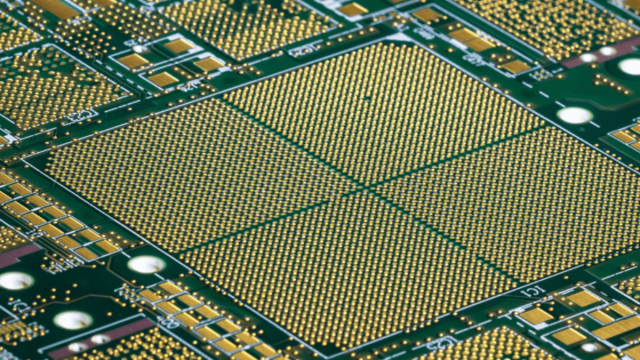
Printed Circuit Boards (PCBs) are the backbone of modern electronics, serving as the platform for connecting and interconnecting various electronic components. As technology advances, the demand for smaller, more efficient, high-performance electronic devices has grown. High-density interconnect (HDI) PCBs have emerged as a key solution to meet these demands, offering a host of benefits while also presenting unique design challenges.
HDI PCBs are characterized by their intricate, densely packed layouts with multiple layers of fine-line traces, microvias, and compact component placement. These features contribute to the numerous advantages of HDI PCBs.
1. Miniaturization
Contents
HDI PCBs allow for a substantial reduction in board size, enabling smaller and more portable electronic devices. This is especially important in applications such as smartphones, wearables, and IoT devices, where space constraints are critical.
Circuit design software plays a pivotal role in modern electronics, enabling engineers and hobbyists to bring their innovative ideas to life through the seamless creation and analysis of intricate electronic circuits.
2. Improved Signal Integrity
With shorter trace lengths and controlled impedance, HDI PCBs offer enhanced signal integrity. This is crucial for high-speed data transmission and signal quality, as any interference or signal degradation can result in performance issues.
3. Increased Component Density
HDI technology permits a higher component density, allowing more functionality in a smaller space. This not only reduces the overall footprint of the device but also enhances its capabilities.
4. Enhanced Thermal Management
The compact design of HDI PCBs allows for efficient thermal management. It dissipates heat more effectively, vital for high-power and performance-critical applications.
5. Enhanced Reliability
HDI PCBs typically have better reliability due to reduced electromagnetic interference, fewer solder joints, and improved signal paths. This results in a longer lifespan and reduced maintenance.
However, with the numerous benefits of HDI PCBs come several design challenges:
Cost
Designing and manufacturing HDI PCBs can be significantly more expensive than traditional ones. This is primarily due to the increased complexity of the manufacturing process, requiring advanced technologies and specialized equipment.
Manufacturing Complexity
HDI PCBs involve intricate layer stacking, multiple microvias, and complex routing, making manufacturing more challenging. Designers must work closely with PCB manufacturers to ensure the design can be produced accurately and cost-effectively.
Signal Integrity
Achieving and maintaining signal integrity in HDI PCBs is a major challenge. Designers must consider impedance control, crosstalk, and the potential for interference in such tightly packed boards.
Component Placement
Placing components on an HDI PCB can be complex due to limited space and the need to optimize signal paths. This requires careful consideration and planning.
Testing and Inspection
Inspection and testing of HDI PCBs can be more complicated, as accessing inner layers and microvias is difficult. Ensuring the quality of the final product is essential to avoid costly rework.
Material Selection
The choice of materials plays a crucial role in HDI PCB design. Designers must select materials that provide the necessary electrical, thermal, and mechanical properties while meeting space and cost constraints.
In conclusion, High-Density Interconnect (HDI) PCBs offer many benefits for modern electronic devices, including miniaturization, improved signal integrity, increased component density, enhanced thermal management, and enhanced reliability. However, designing HDI PCBs presents numerous challenges, including cost, manufacturing complexity, signal integrity, component placement, testing and inspection, and material selection.
Collaboration between electronics designers and manufacturers is essential to design HDI PCBs successfully. With proper planning, careful consideration of design constraints, and thorough testing, the benefits of HDI PCBs can be harnessed to create smaller, more powerful, and more reliable electronic devices, ultimately driving innovation in the electronics industry.


